
-
- Products
- Indoor Household Cords
- Appliance Cords
- General Purpose Short-Length Cords
- General Purpose Extension Cords
- Landscape & Decorating Cords
- Bright Color Extension Cords
- Oil-Resistant Extension Cords
- Cold-Flex Extension Cords
- VividFlex Power Cords
- EXTREME All-Weather Cords
- Cord Management
- Task Lights
- Adapters & GFCI Devices
- Where to Buy
- About
- Careers
- Glossary
- Catalog


What Is an FPGA Chip and How Does It Work?
An Fpga Chip is a reconfigurable semiconductor device that can be programmed for specific digital tasks. Unlike a fixed-function processor, it allows engineers to reshape internal hardware after manufacturing. This flexibility makes FPGAs useful in telecommunications, industrial control, medical equipment, automotive systems, and scientific instruments.
Inside an Fpga Chip, configurable logic blocks perform Boolean operations and store temporary results. Programmable routing channels connect these blocks across the silicon. Engineers describe the desired circuit with hardware languages such as VHDL or Verilog. A synthesis tool converts that description into a configuration file. The file then programs lookup tables, flip-flops, memory blocks, and input-output resources. Tiny switches change the signal paths.
That process supports parallel execution. Several operations can run during one clock cycle, often reducing latency in demanding applications. A processor usually follows instructions in sequence. An FPGA can build a pipeline that moves data through multiple stages, like parts moving along a factory line. However, flexibility does not guarantee better performance. Development can require specialized knowledge, careful timing analysis, and repeated hardware testing.
Real projects also expose practical limitations. An FPGA may consume more power than a custom chip for the same task. It can cost more than a microcontroller in simple designs. The comparison is not always clean. Device families differ greatly in speed, memory, power use, and software support. Understanding how an Fpga Chip works therefore requires more than memorizing its architecture. It requires examining the design goal, workload, operating environment, and evidence from actual measurements.
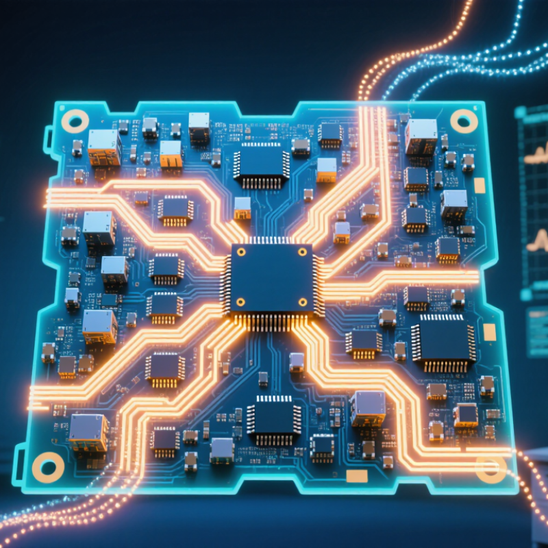
Table of Contents [Hide]
FPGA Chip Definition and Core Characteristics
What Is an FPGA Chip and How Does It Work?
FPGA Chip Definition and Core Characteristics
An FPGA, or field-programmable gate array, is a semiconductor device configured after manufacturing. Unlike a fixed circuit, it can be rewired for a specific task. Its internal structure usually includes configurable logic blocks, routing channels, memory elements, and input/output circuits. Small lookup tables perform logic operations, while flip-flops store values on clock edges. These parts work together through programmable connections.
Engineers describe the design with hardware languages, then convert it into a configuration file called a bitstream. The bitstream sets logic functions and routing paths inside the chip. For example, an FPGA can receive sensor samples, process several values in parallel, and send results within predictable clock cycles. This parallel structure often reduces latency. It also supports hardware updates without redesigning the physical circuit.
Flexibility is a core characteristic, but it is not unlimited. Available logic cells, memory, pins, and routing resources constrain the design. Timing closure can become difficult when signals travel across a crowded layout. Power use may also increase when many circuits switch simultaneously. I once treated reconfigurability as an automatic advantage, but that view was incomplete. A poorly planned design can waste resources and perform worse than a simpler circuit. Careful clock planning, simulation, and hardware testing remain essential. Real measurements matter.