
-
- Products
- Indoor Household Cords
- Appliance Cords
- General Purpose Short-Length Cords
- General Purpose Extension Cords
- Landscape & Decorating Cords
- Bright Color Extension Cords
- Oil-Resistant Extension Cords
- Cold-Flex Extension Cords
- VividFlex Power Cords
- EXTREME All-Weather Cords
- Cord Management
- Task Lights
- Adapters & GFCI Devices
- Where to Buy
- About
- Careers
- Glossary
- Catalog


How to Choose Monolithic Integrated Circuits?
Choosing a Monolithic Integrated circuit begins with the application, not the part number. A compact package may look attractive, yet thermal limits, noise, supply variation, and lifecycle risks can change the decision. WSTS forecast global semiconductor sales at approximately $611 billion in 2024, following a difficult 2023. This scale reflects strong demand, but it also exposes buyers to broader product choices and uneven availability.
A practical selection process starts with the datasheet. Check operating voltage, load current, frequency range, input and output limits, accuracy, package thermal resistance, and qualification status. For automotive or industrial equipment, AEC-Q100 documentation, temperature grades, and production traceability deserve close attention. A circuit that works on a laboratory bench may fail inside a sealed enclosure at 85°C. The margins matter.
Industry reports from WSTS and the Semiconductor Industry Association show continued semiconductor investment and expanding application requirements. However, market growth does not guarantee long-term support for every device. Verify the manufacturer’s product-change notifications, estimated longevity, authorized distribution, and second-source options. Compare total cost, not only unit price. Board area, external components, assembly time, and field-service exposure all influence value.
My first filter is often wrong. I may favor higher specifications when a simpler device offers better stability and availability. That is why prototypes, worst-case calculations, and thermal measurements should confirm the final choice. The best Monolithic Integrated solution balances electrical performance, manufacturability, compliance, supply continuity, and realistic operating conditions. There is no universal winner. The right device is the one that remains dependable after the enclosure closes.
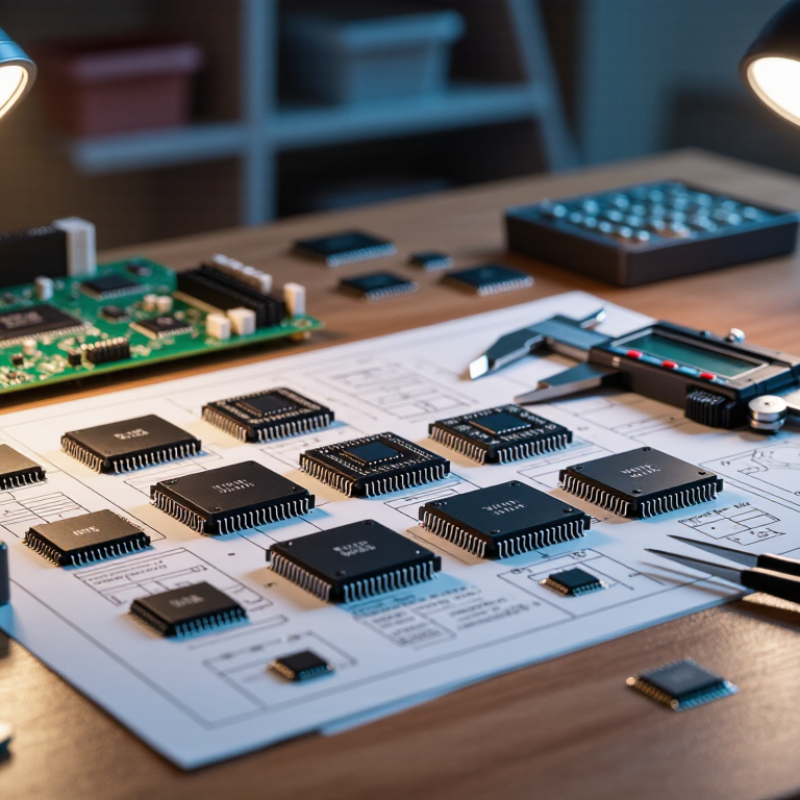
Table of Contents [Hide]
What Monolithic Integrated Circuits Are and How They Function
A Monolithic Integrated Circuit is a complete electronic circuit formed on one semiconductor die. The die usually contains transistors, resistors, capacitors, and tiny metal connections. These elements work together inside a small package.
Unlike a circuit built from separate components, a monolithic IC shortens signal paths and improves consistency. Digital versions process binary signals through switching transistors. Analog versions manage changing voltages, currents, or sensor signals. Mixed-signal devices perform both tasks. In operation, power enters through dedicated pins, while internal structures control, amplify, compare, store, or convert signals. Heat still matters. A small package can become surprisingly warm under continuous load.
When choosing an IC, match its function with the circuit’s real conditions. Check operating voltage, output current, frequency range, temperature limits, package type, and input thresholds. Read the electrical specifications carefully, not only the product description. In practical testing, two circuits can behave differently because of wiring length, noise, or an overlooked load. I have found that a technically suitable IC may still perform poorly when its grounding is weak. That detail is easy to underestimate.
Tips: Sketch the signal path before selecting the device. Leave voltage margin around the normal supply level. Compare typical and maximum values. Test the circuit under heat and low-voltage conditions. Datasheets are reliable, but real measurements can reveal assumptions you missed. The first choice is not always the best one.